- 您现在的位置:买卖IC网 > Sheet目录320 > DC1597A (Linear Technology)BOARD EVAL LTM8031
�� �
�
�LTM8031�
�APPLICATIONS� INFORMATION�
�GND�
�C� OUT�
�AUX�
�BIAS�
�FIN�
�SYNC�
�RUN/SS�
�V� IN�
�OPTIONAL�
�FIN�
�CAPACITOR�
�V� OUT�
�C� IN�
�GND�
�8031� F03�
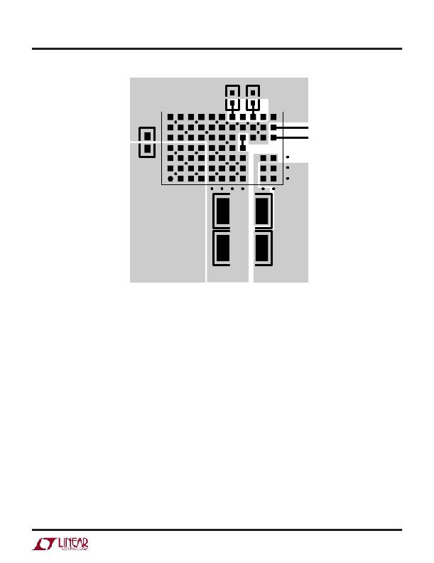
�Figure� 3.� Layout� Showing� Suggested� External� Components,�
�GND� Plane� and� Thermal� Vias�
�4.� Place� the� C� IN� and� C� OUT� capacitors� such� that� their�
�ground� currents� flow� directly� adjacent� or� underneath�
�the� LTM8031.�
�5.� Connect� all� of� the� GND� connections� to� as� large� a� copper�
�pour� or� plane� area� as� possible� on� the� top� layer.� Avoid�
�breaking� the� ground� connection� between� the� external�
�components� and� the� LTM8031.�
�6.� Use� vias� to� connect� the� GND� copper� area� to� the� board’s�
�internal� ground� plane.� Liberally� distribute� these� GND� vias�
�to� provide� both� a� good� ground� connection� and� thermal�
�path� to� the� internal� planes� of� the� printed� circuit� board.�
�Hot-Plugging� Safely�
�The� small� size,� robustness� and� low� impedance� of� ceramic�
�capacitors� make� them� an� attractive� option� for� the� input�
�bypass� capacitor� of� LTM8031.� However,� these� capacitors�
�can� cause� problems� if� the� LTM8031� is� plugged� into� a� live�
�or� fast� rising� or� falling� supply� (see� Linear� Technology�
�Application� Note� 88� for� a� complete� discussion).� The� low�
�loss� ceramic� capacitor� combined� with� stray� inductance� in�
�series� with� the� power� source� forms� an� under-damped� tank�
�circuit,� and� the� voltage� at� the� V� IN� pin� of� the� LTM8031� can�
�ring� to� twice� the� nominal� input� voltage,� possibly� exceed-�
�ing� the� LTM8031’s� rating� and� damaging� the� part.� A� similar�
�phenomenon� can� occur� inside� the� LTM8031� module,� at� the�
�output� of� the� integrated� EMI� filter,� with� the� same� potential�
�of� damaging� the� part.�
�If� the� input� supply� is� poorly� controlled� or� the� user� will� be�
�plugging� the� LTM8031� into� an� energized� supply,� the� input�
�network� should� be� designed� to� prevent� this� overshoot.� Fig-�
�ure� 4� shows� the� waveforms� that� result� when� an� LTM8031�
�circuit� is� connected� to� a� 24V� supply� through� six� feet� of� 24-�
�gauge� twisted� pair.� The� first� plot� (4a)� is� the� response� with�
�a� 2.2μF� ceramic� capacitor� at� the� input.� The� input� voltage�
�8031fb�
�13�
�发布紧急采购,3分钟左右您将得到回复。
相关PDF资料
DC1693A
BOARD DEMO FOR LTM8047
DC1696A
BOARD DEMO FOR LTM8026
DC1724A
BOARD EVAL LTM8029
DCATV
SURGE SUPPRESSOR F COAX
DD1P030MA1
CONN PLUG 30POS 0.5MM
DD2P040MA1
CONN PLUG 40POS 0.5MM
DEIC421
RF MOSFET DRIVER 20 AMP
DEMO56F8013-EE
BOARD DEMO FOR 56F8013
相关代理商/技术参数
DC15B
制造商:FLORIDA MISC. 功能描述: 制造商:Florida Misc. 功能描述:
DC-15B
制造商:FLORIDA MISC. 功能描述: 制造商:Florida Misc. 功能描述:
DC-15FB
制造商:Pan Pacific 功能描述:
DC15KV
制造商:MURATA 制造商全称:Murata Manufacturing Co., Ltd. 功能描述:High Voltage Ceramic Capacitors (over 10kV)
DC-15MB
制造商:Pan Pacific 功能描述:
DC15PTE
制造商:NORTHERN TECHNOLOGI 功能描述:CONNECTOR
DC15ST
制造商:Northern Technologies Corporation 功能描述:
DC1600
制造商:INTRONICS 制造商全称:INTRONICS 功能描述:15 Watt Triple Output DC-DC Converters